Interfacing to an LCD module
using bus functions
Submitted by:
The programs and drawings shown below are taken from the examples section
of the manual.
The example for controlling LED's is similar to this example in that
the goal is to display visual information to the user of the application.
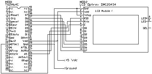
In this example we are connecting the TICkit 62 to an LCD module based
on the popular Hitachi 44780 chip set. Most of the LCD alpha-numeric displays
on the market use this chip set and it has become the dominant defacto
standard for displays up to 4 lines by 40 characters. These modules are
usually available for $10 or less from surplus outlets like B.G. Micro.

These modules are available with special electronics made by Scott Edwards
Electronics and others which allow them to be interfaced serially. This
example does not use any additional electronics and interfaces to the TICkit
via a 4 bit serial bus connection. The direct connection is a more versatile
in that it allows reading of the modules memory as well as writing to it.
This is handy for scrolling and other effects. These modules can be connected
by either a 4 bit or an 8 bit bus, but to conserve I/O we sacrifice some
speed of bus transfer to retain pins D0 through D3 for other uses. The
circuit for this example is shown above.
The key to this type of module is understanding its internal architecture and command format. We will discuss that next, but first we need to discuss
the TICkit bus emulation routines. There are three routines available in
the TICkit 62 for using the general purpose pins in a bus simulation. As
you might imagine, the D-pins are used for the data lines of the bus, and
the A pins are used for address lines. The function buss_setup() is used
to tell the TICkit which of the address lines will be used for bus functions
and which are free for general purpose use. The buss_setup() function also
specifies which data lines are used, either all 8 pins or only the top
4 are used by the bus simulation. An additional option is available, if
only 4 bits of data lines are used. That option is a single or double nibble.
The LCD module can use a 4 bit double nibble bus method instead of an 8
bit bus to transfer 8 bits worth of data.
The bus simulation can only use address lines 0 through 5 for actual
address lines, pin A6 is used as a Read/Write control line and pin A7 is
reserved for download purposes. There is also a subtle difference between
pins A0-A2 and pins A3-A5. When the bus is idle or between operations,
all the address lines go to zero. To prevent false writes or reads to multiple
registers in a single device, pins A3-A5 go to zeros first. This causes
any selected device to become un-enabled, then pins A0-A2 can change with
no effect. This method of bus interface is similar to Rockwell's or Motorola's
method. It means that there is a device enable and reading/writing is controlled
by a single read/write line.

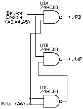
The other common type of bus interface is the Intel or Zilog method
where a separate line is used for /write and for /read. These pins can
be derived from the select logic and the R/W pin to generate the desired
signals. A logic diagram for this is shown above with this example's schematic.
Now lets take a closer look at the LCD module's electronics and architecture.
Whether the display is 2 x 40 or 4 x 16 or any line-column configuration
in between, the internals of the module are the same. The display memory
is organized as one line at addresses x00 to x27 and the second line at
0x40 to 0x67. If the display has 4 lines, the display memory for the first
line is split between the first and third line, while the display memory
for the second line is split between the second and forth line. This makes
writing specific display positions and scrolling the display arcane, but
it is doable none the less.

In addition to the 160 bytes of display data RAM (DD RAM), there are
64 bytes of user programmable character generator RAM. If the display is
programmed for 5x7 characters, this comes out to 8 custom characters. If
the display is programmed for 5x10 characters, there are only 4 custom
characters available. The table that follows shows the mapping of the character
generator RAM (CG RAM) when in 5x7 character mode.
Only the pattern for two of the eight possible custom characters is
shown, but the method should be clear from these two examples. The two
characters are programmed for an 'H' and the small letter 'g' to demonstrate
a descender.
Character Codes
(as in DD RAM)
7 6 5 4 3 2 1 0
|
CG RAM addresses
(for programming)
7 6 5 4 3 2 1 0
|
Character Pattern
(as in CG RAM)
7 6 5 4 3 2 1 0
|
0 0 0 0 * 0 0 0
|
0 0 0 0 0 0 0 0
|
X X X 1 0 0 0 1
|
|
0 0 0 0 0 0 0 1
|
X X X 1 0 0 0 1
|
|
0 0 0 0 0 0 1 0
|
X X X 1 0 0 0 1
|
|
0 0 0 0 0 0 1 1
|
X X X 1 1 1 1 1
|
|
0 0 0 0 0 1 0 0
|
X X X 1 0 0 0 1
|
|
0 0 0 0 0 1 0 1
|
X X X 1 0 0 0 1
|
|
0 0 0 0 0 1 1 0
|
X X X 1 0 0 0 1
|
|
0 0 0 0 0 1 1 1
|
X X X 0 0 0 0 0
|
0 0 0 0 * 0 0 1
|
0 0 0 0 1 0 0 0
|
X X X 0 0 0 0 0
|
|
0 0 0 0 1 0 0 1
|
X X X 0 0 0 0 0
|
|
0 0 0 0 1 0 1 0
|
X X X 0 1 1 1 1
|
|
0 0 0 0 1 0 1 1
|
X X X 1 0 0 0 1
|
|
0 0 0 0 1 1 0 0
|
X X X 1 0 0 0 1
|
|
0 0 0 0 1 1 0 1
|
X X X 0 1 1 1 1
|
|
0 0 0 0 1 1 1 0
|
X X X 0 0 0 0 1
|
|
0 0 0 0 1 1 1 1
|
X X X 0 1 1 1 0
|
There are two addressable registers in a 44780 based module. These are
the command register and data register. As you would expect, the data register
is used to read or write data to the DDRAM or CGRAM. The control register
is less obvious. Reads from the control register return a busy flag in
bit 7 and the current address counter (DDRAM pointer) in bits 0 thru 6.
The table that follows summarizes the command structure:
Instruction
name
|
Control
RS R/W
|
Data Bits
7 6 5 4 3 2 1 0
|
Description
|
Clear Display
|
0 0
|
0 0 0 0 0 0 0 1
|
Clears display and
 returns cursor to home
 position (address 00)
|
Return Home
|
0 0
|
0 0 0 0 0 0 1 X
|
Places cursor at
 address 00. Also
 un-shifts display
|
Entry Mode
|
0 0
|
0 0 0 0 0 1 I S
|
Sets the cursor
movement direction.
I=1 inc, I=0 dec,
S=0 no shift,
S=1 shift display.
|
Display Control
|
0 0
|
0 0 0 0 1 D C B
|
Turn Display on (D),
Turn Cursor on (C),
Blink Cursor on (B).
|
Cursor & Display
Shifting
|
0 0
|
0 0 0 1 D R X X
|
Controls shifting and
cursor movement.
D=1 shift display,
 D=0 cursor move,
R=1 shift right,
R=0 shift left.
|
Interface &
 Format
|
0 0
|
0 0 1 D L F X X
|
Controls data bus
width and
display format.
D=1 8 bit bus,
D=0 4 bit bus,
double lines (L),
Large Font (F)
|
Set CG RAM
 Address
|
0 0
|
0 1 A A A A A A
|
Sets the address for
 CG RAM reading and
 Writing. Subsequent
 read and writes to
 data register affect
 CG RAM contents.
|
Set DD RAM
 Address
|
0 0
|
1 A A A A A A A
|
Sets the address for
 DD RAM reading and
 Writing. Subsequent
 read and writes to
 data register affect
 DD RAM contents.
|
Read Status
|
0 1
|
B A A A A A A A
|
Reads 44780 status.
B=busy processing,
AAAAAAA = address
 count; either DD or CG
 RAM address.
|
Write Data
|
1 0
|
Data to Write
|
Either DD or CG data
|
Read Data
|
1 1
|
Data Read
|
Either DD or CG data
|
The program which follows a specific sequence of commands to
initialize the display. A specific command write timing pattern is necessary
to ensure the display initializes properly. Click an029.zip
to download this program.
DEF tic62_c
LIB fbasic.lib

DEF xbuss_mask 0y00100001b   ; These are the address lines used
DEF lcd_data_reg 0y00100001b ; Address of data register
DEF lcd_cont_reg 0y00100000b ; Address of control register

FUNC none lcd_init
BEGIN
    buss_setup( +( xbuss_mask, buss_4bit ))  ; setup buss for 4bit
    delay( 15 )                              ; wait 15ms
    buss_write( lcd_cont_reg, 0y00110000b )
    delay( 5 )
    buss_write( lcd_cont_reg, 0y00110000b )
    delay( 1 )
    buss_write( lcd_cont_reg, 0y00110000b )
    buss_write( lcd_cont_reg, 0y00100000b )  ; turn it into 4two
    buss_setup( +( xbuss_mask, buss_4two ))

    buss_write( lcd_cont_reg, 0y00101000b )  ; assumes 2 line 5x7 font
    buss_write( lcd_cont_reg, 0y00001111b )
    buss_write( lcd_cont_reg, 0y00000001b )
    buss_write( lcd_cont_reg, 0y00000110b )
ENDFUN
FUNC none lcd_cont_wr
    PARAM byte in_val
BEGIN
    WHILE >=( buss_read( lcd_cont_reg ), 0y10000000b )
    LOOP         ; delay until not busy

    buss_write( lcd_cont_reg, in_val )
ENDFUN
FUNC none lcd_data_wr
    PARAM byte in_val
BEGIN
    WHILE >=( buss_read( lcd_cont_reg ), 0y10000000b )
    LOOP         ; delay until not busy

    buss_write( lcd_data_reg, in_val )
ENDFUN
FUNC none lcd_string
    PARAM word in_ptr
    LOCAL word temp_ptr
    LOCAL byte temp_val
BEGIN
    =( temp_ptr, in_ptr )    ; don't affect calling value
    =( temp_val, ee_read( temp_ptr ))
    WHILE temp_val
        lcd_data_wr( temp_val )
        ++( temp_ptr )
        =( temp_val, ee_read( temp_ptr ))
    LOOP
ENDFUN
FUNC none lcd_out
    PARAM word lcd_data
    LOCAL word place 10000w
    LOCAL word num
BEGIN
    =( num, lcd_data )
    REPEAT
       lcd_data_wr( +( '0', trunc_byte( /( num, place ))))
       =( num, %( num, place ))
       =( place, /( place, 10b ))
   UNTIL ==( place, 0b)
ENDFUN
FUNC none main
    LOCAL word lcount 0
BEGIN
    delay( 500 )       ; wait for 1/2 second for power to settle
    lcd_init()
    lcd_cont_wr( 0y00000001b )   ; Reset the LCD for good measure
    lcd_string( "Hello World..." )
    lcd_cont_wr( 0y11000000b )   ; position to first char on line 2
    lcd_string( "Loop Count: " )
    REP
        lcd_cont_wr( 0y11001100b ) ; 12th char on line 2
        lcd_out( lcount )
        ++( lcount )
    LOOP
ENDFUN
This program just initializes the display, says "Hello World..."
and counts loops on the second line of the display. A simple program, but
a good basis for working with these very versatile LCD modules. There are
additional LCD functions contained on the release disk for you to look
over.
Protean Logic Inc. Copyright 05/06/04
Top of Page


