Submitted by:
Glenn Clark
VersaTech Electronics
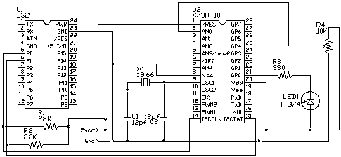
Parallax's Basic STAMP II has proved to be a very capable processor for a wide variety of tasks. Often STAMP based products require additional I/O capabilities, or the ability to perform tasks in background while it continues processing a foreground task. The I2C Xtender 73, made by Protean Logic Inc., can provide these capabilities with a minimum of additional components.
The Xtender can converter analog inputs to 8bit values for measuring voltages, etc. It can also generate PWM signals for motor control or servo control. It can count input pulses for measuring frequencies or RPM. It can control a stepper motor. It has 8 additional general purpose I/O pins. It has 128 bytes of RAM memory. And it can send and receive RS232 serial data.
The sample code below reads the version number of the Xtender, blinks an LED connected to GP0 on the Xtender 128 times, then reads and reports the voltage on the AN0 pin of the Xtender. The A/D value is 8 bit and ratio metric to 5 volts (Xtender Supply) so the granularity of the conversion result is 1=0.195 volts.
Consult the data sheet on the Xtender for more details on the control registers and capabilities of the Xtender.
' Sample routines to do I2C on a STAMPII and an Xtender
' Special Thanks to Victor Epand

xtn_dev  CON $80        ' address for xtender device 0
xtn_reset CON $9e       ' reads current revision and resets xtender
xtn_pins_out CON $9d    ' make GP pins outputs as specified by data_byte
xtn_pins_low CON $9b    ' make GP pins output a low
xtn_pins_high CON $9c   ' make GP pins output a high
xtn_ad_cont CON $82     ' A/D control register
xtn_ad_res CON $82      ' reads from this register are results of last conv.

b var byte      ' temp storage for demo program

main_prog:
    input si2c_data
    input si2c_clk      ' initial state

    ' Show revision of the Xtender and prove communications
    debug "Extender Revision:"
    addr_byte=xtn_dev
    comm_byte=xtn_reset
    gosub si2c_read
    debug dec data_byte, CR
    pause 3000

    ' Blink a light for a while
    addr_byte=xtn_dev
    comm_byte=xtn_pins_out
    data_byte=%00000001         ' only make GP0 an output
    gosub si2c_write

    b=128
    xtn_blink_lp:
        debug "Blinking LED on GP0", CR
        comm_byte=xtn_pins_high
        gosub si2c_write
        pause 50
        comm_byte=xtn_pins_low
        gosub si2c_write
        pause 50
        b = b + 1
        IF b then xtn_blink_lp

    ' read channel one of the A/D
    debug "Reading A/D channel 0", CR
    xtn_adread_lp:
        addr_byte=xtn_dev
        comm_byte=xtn_ad_cont
        data_byte=%00000101   ' channel 0, internal ref, power up
        gosub si2c_write

        comm_byte=xtn_ad_res
        gosub si2c_read
        debug "A/D result: "
        debug dec data_byte, CR
        goto xtn_adread_lp

    end


' Simulated Inter-Integrate Circuit driver (si2c)
' This driver consists of two internal routes (si2c_wbyte and si2c_rbyte)
' and two user functions (si2c_write and si2c_read)
' the si2c_write function needs three byte parameters:
'     addr_byte: the i2c address of the device writing to
'     comm_byte: the sub command to tell the device what to do
'     data_byte: the byte of data to use for the command
'
' the si2c_read function needs two parameters and returns a byte:
'    addr_byte: the i2c address of the device reading from
'    comm_byte: the sub command to tell the device what to read
'    data_byte: the value returned from the device that was read


' This routine used pin 0 as the I2C clock pin and pin 1 as the I2c data pin
' Both of these pins must be pulled high. Both of these pins should initially
' be configured as inputs at power up.

si2c_clk CON 0          ' I/O pin for I2C Clock line
                        ' IN0 is used in some situations
si2c_data CON 1         ' I/O pin for I2C data line
                        ' IN1 is used in some situations

' the following are the storage required by the si2c routines.
in_byte VAR byte        ' used internally by the si2c_wbyte function
bit_count VAR byte      ' used internally by both the si2c_wbyte and rbyte
send_ack VAR bit        ' used to tell rbyte if it should ack or not
exit_ack VAR bit        ' used to indicate if wbyte got an ack or not
data_byte VAR byte      ' either the data to be written or the data just read
addr_byte VAR byte      ' address of I2C device (LSB=read indicator)
comm_byte VAR byte      ' I2C sub command

si2c_wbyte:             ' returns 1 if successful, 0 = NACK
                        ' in_byte is byte to be written
    bit_count=%10000000
    si2c_wbyte_lp:
        low si2c_clk
        input si2c_data
        IF (bit_count & in_byte) then si2c_wbyte_do1
            low si2c_data
        si2c_wbyte_do1:
        bit_count=bit_count>>1
        input si2c_clk
        IF bit_count then si2c_wbyte_lp

    ' now test the acknowledge bit
    low si2c_clk
    input si2c_data
    input si2c_clk
    exit_ack=0
    IF in1 then si2c_wbyte_ex
        exit_ack=1
    si2c_wbyte_ex:
    return


si2c_rbyte:             ' send_ack is set for a post ack or not
    bit_count=%10000000
    low si2c_clk
    data_byte=0
    input si2c_data
    si2c_rbyte_lp:
        input si2c_clk
        si2c_rbyte_wt:
            IF in0=0 then si2c_rbyte_wt
        IF in1=0 then si2c_rbyte_dl
            data_byte=data_byte|bit_count
        si2c_rbyte_dl:
        low si2c_clk
        bit_count=bit_count>>1
        IF bit_count then si2c_rbyte_lp

    ' send ack bit if required
    low si2c_data
    IF send_ack then si2c_rbyte_ak
        input si2c_data
    si2c_rbyte_ak:
    input si2c_clk
    return


si2c_write:     ' must set addr, comm, and data before calling
    low si2c_data ' generate a start bit
    si2c_write_lp:
        in_byte=addr_byte
        gosub si2c_wbyte
        IF exit_ack=0 then si2c_write_lp
    in_byte=comm_byte
    gosub si2c_wbyte
    in_byte=data_byte
    gosub si2c_wbyte
    low si2c_clk        ' generate stop bit
    low si2c_data
    input si2c_clk
    input si2c_data
    return


si2c_read:      ' must set addr, comm,  data_byte will have return
    low si2c_data ' generate a start bit
    IF addr_byte.bit0=1 then si2c_read_sk
        si2c_read_lp:
            in_byte=addr_byte
            gosub si2c_wbyte
            IF exit_ack=0 then si2c_read_lp
        in_byte=comm_byte
        gosub si2c_wbyte
        low si2c_clk
        low si2c_data
        input si2c_clk
        input si2c_data ' generate the stop
        low si2c_data   ' generate a start
        addr_byte=addr_byte+1
    si2c_read_sk:
    in_byte=addr_byte
    gosub si2c_wbyte
    send_ack=0
    gosub si2c_rbyte
    low si2c_clk
    low si2c_data
    input si2c_clk
    input si2c_data     ' generate the stop bit
    return
Protean Logic Inc. Copyright 05/06/04 Top of Page